
[Deep Dive Research] Back-End Semiconductor Equipment: The Fields Have Grown. One Seed Spot Remained.

Buongiorno. 🌱
This deep dive covers back-end semiconductor equipment. The sector has already run hard. The obvious question writes itself.
Is the party already over?
We also saw 30–40% single-day moves in some names over the past two days. The timing may feel awkward. But we wanted to check whether anything still looks interesting — and whether the names that have gotten all the attention are actually fairly priced.
Is the Party Already Over?
Back-end equipment stocks have been rising steadily for one to two years. At first glance, the chart suggests it might be too late.
We decided not to take that at face value. Three questions had to be answered first.
Is the memory shortage real? Will capital spending into back-end continue through 2027? And does the cycle hold together beyond 2028?
On the memory shortage: We addressed this a month ago in our memory check-up piece. SK Hynix and Samsung both said explicitly in their IR communications that this cycle is structurally different from past ones. Samsung noted that 2027 demand is already being booked now.
One more data point: DDR4 spot prices are up 1,360% from their 2024 lows. AI data centers are absorbing roughly 70% of global DRAM demand. New fabs take four to five years to build. The 2026–2027 window is structurally incapable of clearing the shortage. Answer: real.
On 2027 CAPEX: TSMC’s 2026 capex is approximately $56 billion — an all-time high. CoWoS capacity is set to quadruple from end-2024 levels. NVIDIA has locked in roughly 60% of 2026 capacity and 50% of 2027. The 10-percentage-point decline isn’t demand softening — it’s AMD, Broadcom, and Google taking their own slices with custom AI chips.
The clearest signal: TSMC outsourced advanced packaging for the first time. Approximately 240,000–270,000 wafers, with 180,000–190,000 going to Amkor. When TSMC runs out of room, the cycle still has legs. Answer: accelerating.
On post-2028: Back-end equipment typically runs six to nine months from order to revenue recognition. If 2028 and beyond were empty, the search for new positions would be less meaningful. The HBM roadmap looks like this: HBM4 in 2026, HBM4E in 2027–2028, HBM5 in 2028–2030, HBM5E around 2031. Each generation requires new equipment cycles. Answer: no cliff.
All three questions passed. But the process surfaced an unexpected clue.
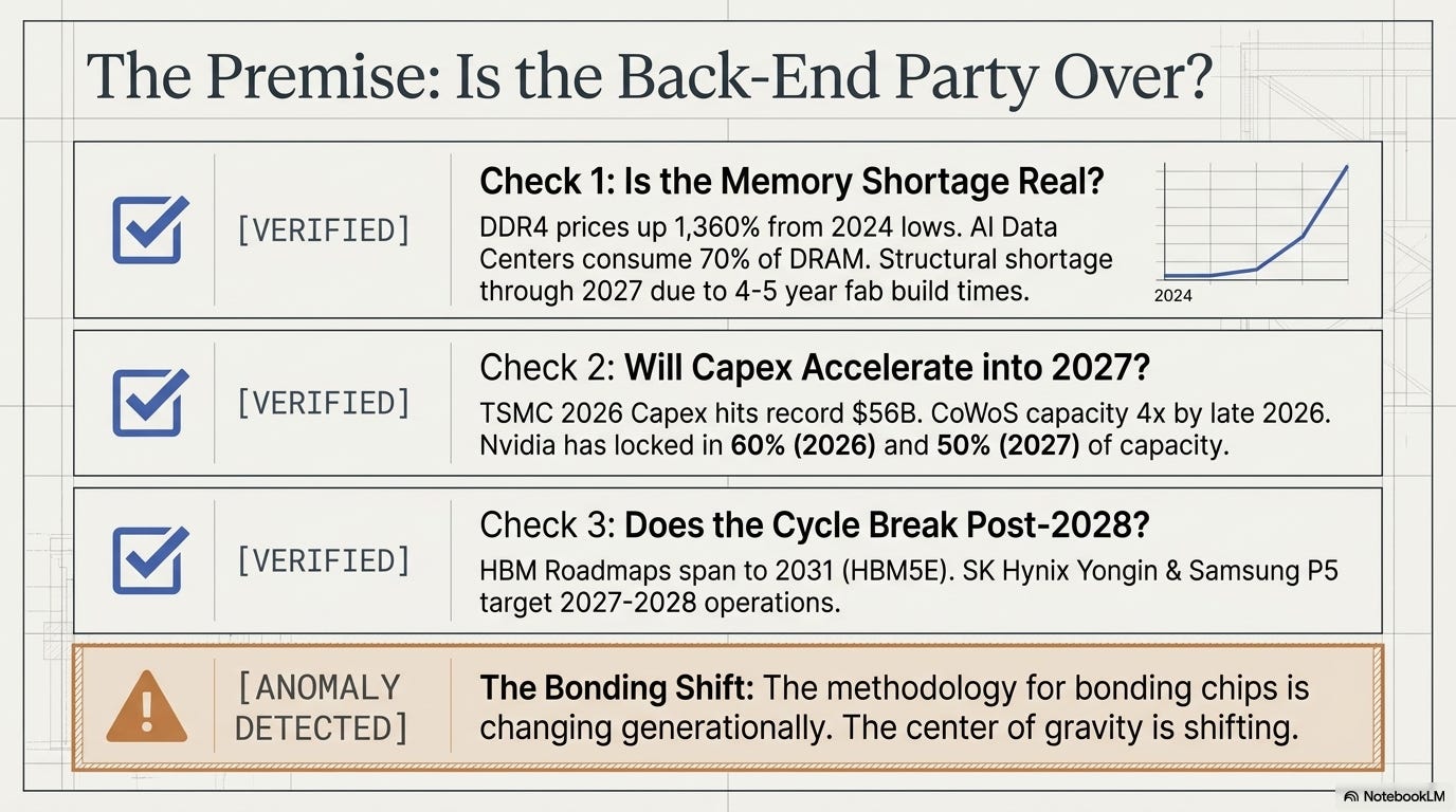
Beyond HBM5, stacking 20-plus layers changes the bonding method entirely. TC bonders — where Hanmi Semiconductor leads — remain the primary tool through HBM4E. The extension came from JEDEC relaxing height limits, giving the existing approach another generation. But beyond that, hybrid bonding takes over: copper-to-copper, no bumps. BESI and ASMPT are better positioned there.
The signals are already in the order data. SK Hynix placed its first mass-production hybrid bonding order in March 2026 — a system jointly developed by AMAT and BESI. Samsung has decided to introduce hybrid bonding starting with HBM4, running parallel qualification with SEMES and BESI equipment.
Hanmi isn’t standing still. It’s investing over ₩50 billion in a dedicated hybrid bonding line at its Incheon Plant 7, targeting a 2027 ramp, and has received a development order from SK Hynix on the technology.
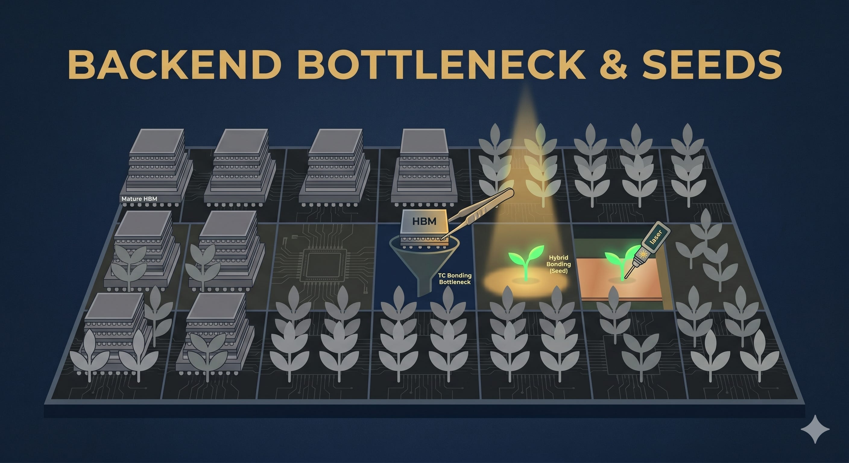
The center of gravity is shifting — but it’s not a displacement story. The bonding pie is getting bigger. The seats inside it are being rearranged.
The party isn’t over. It’s moving to a different room.
What Is Actually Happening in Back-End?
Back-end works differently from front-end.
Our earlier piece on front-end materials concluded: the same fab wears out faster. As processes become more precise, consumables get used up more quickly — recurring revenue on every wafer.
Back-end is different. A single piece of equipment costs tens to hundreds of millions of won. It doesn’t wear out daily. You need to buy more units to add capacity. The right frame here is:
The same chip stays longer.
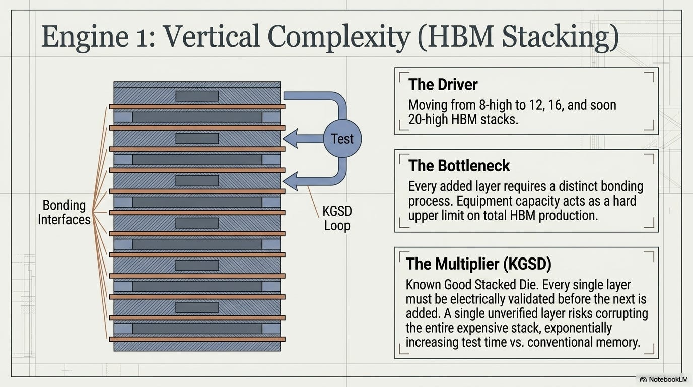
HBM stacking requires bonding at every layer — 12 times for a 12-layer stack, 16 for a 16-layer stack. At each step, there’s a KGSD check (Known Good Stacked Die): confirming that everything stacked so far is functioning correctly. One bad layer makes everything above it worthless. As bonding repeats, so does verification.
Two engines are driving this.
First, HBM stacking itself. More layers, more bonding cycles, more test insertions per die. The throughput ceiling on bonding equipment becomes the ceiling on HBM output.
Second, AI accelerator packaging. NVIDIA’s CoWoS (Chip on Wafer on Substrate) process bonds GPU dies with HBM into a single package. Add SoIC (System on Integrated Chips) on top, and the number of test insertions per advanced AI chip climbs to 10–20. That’s the number Advantest’s CEO cited directly.
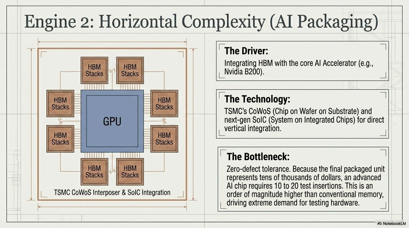
Three pieces of evidence that this is translating into real orders: CoWoS capacity is expanding roughly 4x from end-2024 levels, NVIDIA has locked in the majority of capacity through long-term agreements, and TSMC has opened up outsourcing for the first time. Orders placed today turn into revenue in the second half of 2026 through the first half of 2027. These aren’t stocks that have already priced everything in — they’re companies just beginning to recognize revenue.
Mapping the Back-End Value Chain
Back-end is the sequence of steps between a wafer entering the line and a finished chip coming out. Cut the wafer into dies, stack and bond the dies, heat-treat, surface-flatten, and test electrically.
We mapped nine categories across the process flow. The ★ marks the dominant player in each category.
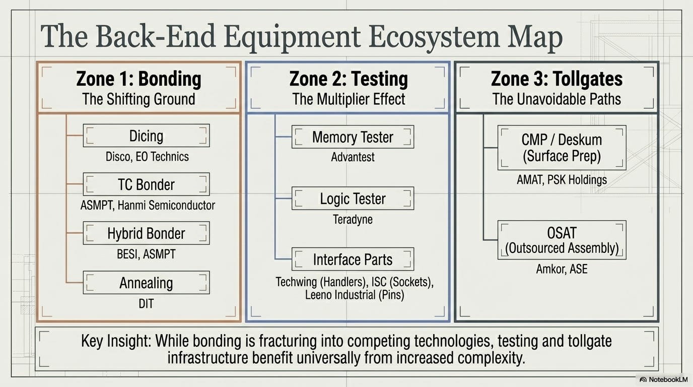
Dicing — cutting wafers into individual dies. Disco (6146 JP) ★ dominates globally. Iotech (039030 KS) has domestic exposure.
TC Bonding — thermal compression bonding, stacking dies with heat and pressure. Primary method through HBM4E. Hanmi Semiconductor (042700 KS) ★ leads domestically. ASMPT (0522 HK) competes globally.
Hybrid Bonding — copper-to-copper direct bonding, no bumps. Primary method from HBM5 onward. BESI (BESI NA) ★ leads globally. ASMPT competes. Hanmi is targeting entry by 2027.
Annealing — post-bonding heat treatment to stabilize the bond interface. DIT (110990 KS) ★ has co-developed with SK Hynix since 2019. Iotech also has exposure.
Descum / CMP — surface planarization before and after bonding. PSK Holdings (031980 KS) ★ is the primary domestic player. AMAT competes globally.
Memory Testers — electrical inspection of HBM and DRAM. Advantest (6857 JP) ★ dominates.
Logic Testers — electrical inspection of GPUs, CPUs, and ASICs. Teradyne (TER US) ★ leads.
Handlers, Sockets, and Pins — interface components between chips and testers. Techwing (089030 KS) ★ makes handlers and cube probers. ISC (095340 KS) ★ makes test sockets. LEENO Industrial (058470 KS) ★ makes test pins.
OSAT — outsourced semiconductor assembly and test. Amkor (AMKR US) ★ is the largest US-headquartered player. ASE competes.
OSAT sits separately — it’s not a single process step but a full outsourcing model for the entire back-end sequence.
A few things stand out from this map.
Bonding splits into two rows. TC bonding is Hanmi’s territory. Hybrid bonding is BESI’s. The center-of-gravity shift from the first chapter shows up right here in the table.
Testing is deeper than it looks. Three of the nine rows are test-related. As inspection frequency increases, every player in this chain benefits together.
Annealing and descum — DIT and PSK Holdings — sit outside bonding and testing. But they’re required regardless of which bonding method wins. More on that shortly.
Row 9 is where TSMC’s outsourced wafers land. Roughly 70% of that volume goes to a single company: Amkor.
Bonding — The Center of Gravity Is Moving
Bonding is the heaviest position in back-end. Every layer added requires one bonding step. The throughput ceiling of bonding equipment is the production ceiling for HBM.
In Q1 2026, Hanmi Semiconductor and BESI moved in opposite directions within the same quarter. Hanmi’s revenue fell 88% quarter-on-quarter. BESI posted 28% year-on-year revenue growth and guided for 30–40% growth in Q2. AMAT — the world’s largest equipment company — acquired approximately 9% of BESI during the same period. The direction became clear.
The underlying story is a shift in bonding method. TC bonding inserts solder bumps between dies to make the connection. Stack beyond 20 layers and even the bump space becomes a constraint. Hybrid bonding eliminates the bumps entirely — copper bonded directly to copper. Thinner stack, faster signal, better thermal dissipation.
TC bonding remains the primary method through HBM4 and HBM4E. The full transition to hybrid bonding is an HBM5 story — 2028 and beyond.
Hanmi isn’t a finished company. JEDEC’s height relaxation gave TC bonding another generation of runway. Hanmi has also introduced next-generation TC bonders targeting HBM5 and HBM6. And it’s building a hybrid bonding line of its own, targeting a 2027 ramp — while holding a development order from SK Hynix on the technology. It’s a dual-track strategy: protect the present, plant a foot in the future.
That said, the market already knows the TC bonding story. A ₩30 trillion market cap is the result of that knowledge. And the HBM5 transition risk is just starting to surface. Known strength and emerging concern coexist in the same ticker.
A note on annealing: DIT has co-developed laser annealing with SK Hynix since 2019. We initially considered it a hidden hybrid bonding beneficiary. On closer review, two things gave us pause.
DIT’s laser annealing is weighted more toward post-ion-implant wafer recovery in next-generation DRAM than toward hybrid bonding void elimination. And the thermal treatment step inside hybrid bonding appears to be converging toward AMAT’s integrated system. The direct hybrid bonding narrative for DIT was overstated.
More significantly: DIT’s core laser annealing technology is currently subject to criminal proceedings. Prosecutors conducted a search and seizure in 2024 on alleged trade secret misappropriation. Indictments followed in 2025, and the trial is ongoing. The outcome could affect the foundation of the growth thesis.
Iotech also has annealing exposure, but its back-end growth axis sits more in laser dicing and debonding. It has begun supplying laser annealing to Samsung lines and debonding tools to TSMC — tracking the dicing-and-debonding path rather than annealing.
Testing — A Real Bottleneck, but the Market Already Knows
Chips are expensive, so they get tested repeatedly. HBM is checked at every stacking step and again after full assembly. An AI accelerator package with multiple HBM units attached — each worth tens of thousands of dollars — cannot afford to discover a defect post-packaging. Ten to twenty test insertions per advanced AI chip. More inspections means more equipment, more sockets, more pins.
Two companies divide the tester market. Advantest (6857 JP) covers memory. Teradyne (TER US) covers logic. Since HBM is memory, Advantest is the more relevant name for the thesis we’re tracing here. The market has already reached the same conclusion.
In the gap between the testers and the chips, Korean companies hold strong positions.
Techwing (089030 KS) makes handlers and cube probers. The cube prober emerged as the critical inspection tool for stacked HBM dies, and Techwing’s stock is up nearly 14x from its lows on that recognition.
ISC (095340 KS) specializes in rubber test sockets. The HBM angle is understood. What the market has not fully priced is the potential extension into next-generation ASIC sockets and photonics testing.
LEENO Industrial (058470 KS) makes test pins. Its strength is stability across a diversified customer and chip base rather than high-beta exposure to any single theme.
Testing has a genuine bottleneck. But it’s a bottleneck the market has already recognized. Advantest is firmly framed as an HBM beneficiary. Techwing has already run 14x. Incremental upside now depends on new triggers or consensus upgrades.
Beyond Bonding and Testing — Where the Tollgates Sit
We flipped the question. Regardless of whether TC bonding or hybrid bonding wins, regardless of which technology becomes dominant — what positions does every participant have to pass through?
PSK Holdings (031980 KS) is one of those positions. Descum is the process that planarizes and cleans the chip surface before and after bonding. The surface has to be clean and flat for bonding to work. That requirement doesn’t disappear with the bonding method. If anything, hybrid bonding — which demands more precise surface contact — makes surface condition more critical, not less. As CoWoS-type advanced packaging scales up, descum demand scales with it. This was our conclusion in the glass substrate deep dive as well — the path led to TSMC and PSK Holdings.
Amkor (AMKR US) is the other tollgate. TSMC outsourced advanced packaging volume for the first time, and roughly 70% of that went to Amkor. TSMC keeps the high-value processes in-house and routes assembly and test to external partners. As long as CoWoS volume grows, the flow to Amkor grows with it. Amkor is also building advanced packaging capacity in Arizona alongside TSMC, positioning itself for the onshoring trend in AI chip supply chains.
Pricing the Bottlenecks
We walked through the bottlenecks process by process. Now we check how much of those bottlenecks are already priced in.
This valuation is a coordinate tool — it shows where the current share price sits relative to scenarios, not when to buy or sell. For companies with clear earnings visibility, think of it as an early preview of individual target prices in future reports. For companies with financial risk, dilution has already been factored in, so numbers may look more conservative than sell-side consensus. That’s intentional.
All companies were classified by business character and layer position into four types, with fair value midpoints and upper bounds derived accordingly. The midpoint reflects a conservative scenario; the upper bound reflects the most aggressive scenario that remains internally consistent.
All prices as of the time of writing. Sorted by distance from the midpoint of the fair value range and upper bound.
Keep reading with a 7-day free trial
Subscribe to Growth Wave to keep reading this post and get 7 days of free access to the full post archives.